service content
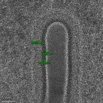
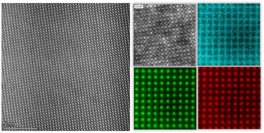
TEM (bright-field images, off-axis dark-field images, center dark-field images, high-resolution images, weak-beam dark-field images); STEM (HAADF images, DF images, BF images, EDS energy spectra, iDPC images); diffraction (selective diffraction, convergent-beam diffraction, nanobeam diffraction)
grade of service
Chip-related sectors (wafer fabs, semiconductor equipment manufacturers, chip design companies, etc.); Materials-related sectors (universities, research institutes, and material R&D enterprises).
Test cycle
Typical processing time: 5-7 working days.
Service Background
With intensified technological blockades abroad, domestic high-tech enterprises are placing greater emphasis on independent chip R&D capabilities, which has fueled a domestic production boom for semiconductor equipment. As chip manufacturing processes continue to shrink, the development of chips and semiconductor equipment increasingly relies on microscopic analytical tools like TEM. Transmission electron microscopy (TEM) plays an irreplaceable role in material research and development. It provides critical microscopic structural information-including crystal structures, defects, elemental compositions, and concentrations-which aids in analyzing material properties and behavior. The technique also
facilitates studies on phase transitions and diffusion processes, offering valuable insights for material design and optimization.
our advantages
Guangdian Metrology specializes in TEM analysis testing technology, boasting an industry-leading expert team and advanced TEM analysis equipment (Talos F200X G2). We provide customized TEM analysis testing solutions tailored to the R&D needs of various clients. Our company possesses FIB-TEM analysis capabilities for advanced processes up to 7nm and below.
case share
Hot Tags: tem imaging and analysis, China tem imaging and analysis service provider, failure analysis, ion cleanliness testing, aec q101 certification test for semiconductor discrete devices, screening of electronic components, aec q200 product test of resistance capacitance inductances and other components, aec q102 product test of optoelectronic devices