Service Content
Advanced Process Chip Analysis
Service Scope
Comprehensive analysis of the metal layers, M0 layers, FinFET structures, etc., of 7nm and below advanced process chips manufactured and designed by chip manufacturing and design companies. This analysis is used to verify the stability of advanced process technologies and key process nodes, and can also be used for competitor analysis and reverse engineering.
Service Background
As integrated circuit manufacturing processes continue to improve, the numbers representing key process nodes are getting smaller and smaller, such as from 65nm and 40nm processes to 22nm, 14nm, 7nm, 4nm, and 3nm processes. Smaller node numbers indicate more advanced processes, meaning better crystal management integration, faster processing speeds, and lower power consumption; however, it also means increased complexity of the chip's internal structure, smaller key structural dimensions, and a gradual development towards nanoscale dimensions that cannot be observed by general microscopic imaging techniques (such as optical microscopes).
Because TEM samples need to be very thin for electrons to penetrate and form diffraction patterns, FIB's efficient sputtering allows for fine processing of samples; therefore, FIB is often used for optimizing the preparation of ultrathin TEM samples.
Our Advantages
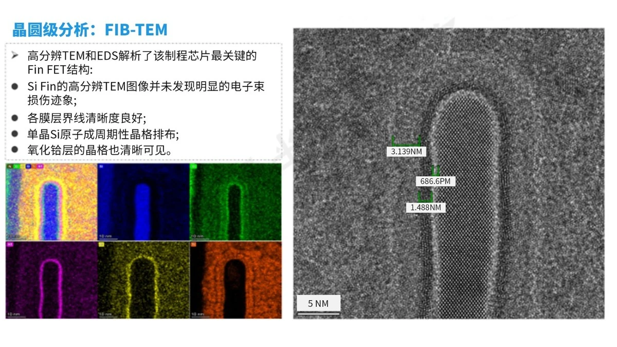
GRGTEST Metrology possesses patented technologies including methods for eliminating the curtain effect of the FIB focused ion beam, a novel framework structure method for preparing heat-sensitive TEM ultrathin samples using DB FIB, a FIB step-thinning method for preparing ultrathin TEM samples of brittle and easily cracked materials, a focused ion beam ultrathin sectioning pretreatment method for radiation-sensitive fine-structure wafer samples, and a method for preparing TEM samples using FIB inverted cutting. These technologies enable high-resolution TEM images with no electron beam damage, achieving atomic-level resolution morphological characterization and compositional analysis of advanced process chips.
Case Study
Chip FA Analysis - 3D TEM Method
Hot Tags: advanced fib & tem for wafers analysis, China advanced fib & tem for wafers analysis service provider, screening of electronic components, aec q200 product test of resistance capacitance inductances and other components, aec q101 certification test for semiconductor discrete devices, ion cleanliness testing, failure analysis, aec q102 product test of optoelectronic devices