

The emergence of advanced process technologies such as copper pillar interconnects has significantly propelled the three-dimensional miniaturization of modern electronic devices and accelerated performance enhancements in related equipment. However, this progress has introduced challenges in failure analysis for advanced packaging technologies. For advanced packaging applications, failure localization may require processing depths exceeding 100 μm, where traditional Gallium ion (Ga⁺) Focused Ion Beam (FIB) struggles to achieve rapid defect localization.
This limitation arises because Ga⁺ FIB operates at a maximum beam current of ~100 nA under 30 keV, requiring tens of hours to process a 500 μm² area. In contrast, Plasma FIB (PFIB) utilizes Xenon ions (Xe⁺) as the ion source, delivering a maximum beam current of ~2.5 μA at 30 keV-over 20 times more efficient than Ga⁺ FIB. This breakthrough enables PFIB to overcome the bottleneck of traditional Ga⁺ FIB: rapid large-area processing.
PFIB Application Case Studies
① TSV Cross-Sectional Morphology and EBSD Crystal Orientation Analysis
Leveraging PFIB's high-speed large-volume cross-sectioning capability, rapid and precise cross-sectional morphology analysis can be performed on Through-Silicon Vias (TSV)-a critical structure in 2.5D/3D advanced packaging. Concurrently, crystal orientation analysis of the cross-section can be conducted using an external Electron Backscatter Diffraction (EBSD) probe, as illustrated in Figure 1.
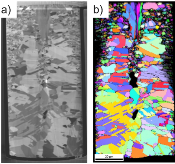
*Figure 1. a) Cross-sectional SEM image of TSV (Through-Silicon Via), a key structure in 2.5D/3D advanced packaging;
b) EBSD analysis (IPF-Y mapping) (Images courtesy: Thermo Fisher Scientific).*
② Large-Area Ultra-Thin TEM Sample Preparation for 3D NAND (Planview Sampling)
Another critical function of PFIB is the preparation of large-area ultra-thin transmission electron microscopy (TEM) samples. GRGTEST now achieves site-specific TEM sample preparation with lengths and widths exceeding 50 μm, meeting the requirements for atomic-resolution TEM observation.
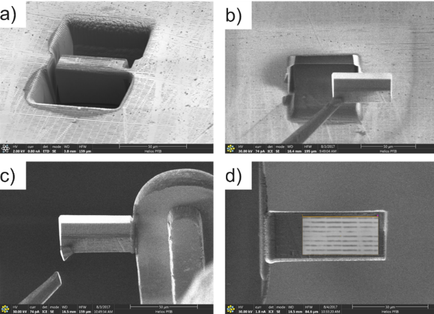
*Figure 2. Process flow for large-area ultra-thin TEM sample preparation (Sample: 3D NAND; Planview extraction size ~50 μm):
a) Trench milling; b) Lift-out and extraction; c) Transfer to TEM grid; d) Final thinning.*
GRGTEST PFIB Service Capabilities
The PFIB system at GRGTEST's Wuxi IC Testing and Analysis Laboratory is the state-of-the-art Thermo Fisher Scientific Helios 5 PFIB system, currently the most advanced Xe-FIB platform in the market. It achieves SEM imaging resolution below 1 nm, with optimized ion beam performance and automation compared to its predecessor (Helios G4 DualBeam). Equipped with a nanomanipulator, Gas Injection System (GIS), and Energy-Dispersive X-ray Spectroscopy (EDX) probe, GRGTEST's PFIB addresses both fundamental and advanced semiconductor failure analysis needs.