

Under the trend of high-density, multi-layer microelectronic packaging, components such as chips, substrates, and connectors are prone to warpage deformation due to CTE (Coefficient of Thermal Expansion) mismatch during high-temperature processes (e.g., reflow soldering) or operational conditions. This can lead to critical failures like solder joint cracking and interface delamination. How can deformation risks be quantitatively assessed? Thermal warpage testing provides the key data support!
1. GRGTEST Thermal Warpage Testing
Utilizing shadow moiré technology, our solution captures dynamic deformation of components under high temperatures with 1μm-level precision, helping you:
- Pinpoint failure root causes: Applicable to chip packaging, substrates (PCB/ceramic/silicon), and connectors, quickly identifying warpage-exceeding zones.
- Simulate real high-temperature scenarios: Supports testing from room temperature to 260°C (e.g., RT→220°C heating, 260°C→RT cooling), replicating critical conditions like reflow soldering and high-temperature operation.
- Data-driven process optimization: Delivers 3D deformation maps + quantitative warpage reports, providing scientific support for material selection, structural design, and process parameter adjustments.
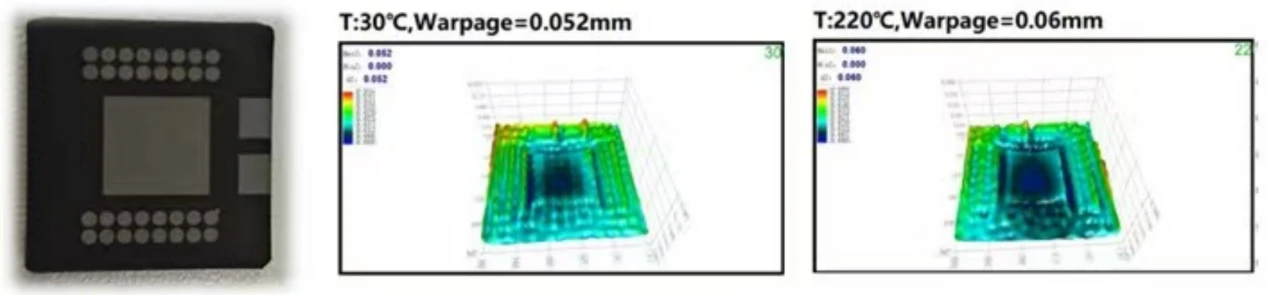
2. GRGTEST Thermal Warpage Testing Capabilities
GRGTEST's IC Testing & Analysis Lab is equipped with the industry-leading TOPWM-HFA4V3.0 "Shadow" Moiré Warpage Testing System, one of the most advanced thermal warpage measurement solutions available.
- Sub-micron resolution with a 350×350mm large-sample testing capacity, significantly expanding detection range compared to previous-gen systems.
- Integrated in-situ thermal stage supporting ultra-fast heating at 1.5°C/s, accurately simulating various reflow soldering temperature profiles and meeting JEDEC-standard thermal stress analysis requirements.
- Special spray coating technology resolves imaging challenges for high-reflectivity/transparent samples, while Matlab-based 3D surface reconstruction algorithms automatically extract full-dimensional data (including curvature, deformation vectors, etc.), generating customized analytical reports.
GRGTEST continues to expand its semiconductor metrology capabilities, now offering thermal warpage analysis at wafer, device, and substrate levels, delivering end-to-end surface deformation testing solutions from R&D to mass production.