In a significant milestone for China's semiconductor industry, domestic brands have achieved a major breakthrough in the independent R&D and design of 3nm process smartphone processor chips, as recently reported by China Central Television (CCTV).
This advancement narrows the gap with international leaders, breaks long-standing technological monopolies, and drives synergistic upgrades across the domestic semiconductor supply chain, including packaging & testing and materials supply.

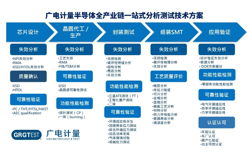
GRGTEST has established comprehensive technical service capabilities for quality evaluation and reliability enhancement across the entire semiconductor industry chain. Holding industry-leading numbers of CNAS and CMA-accredited inspection and analysis programs, GRGTEST provides full-process analysis and verification services – spanning design validation, wafer manufacturing, packaging & testing, SMT assembly, and application validation. This covers the entire product lifecycle "from design to end-product." Crucially, GRGTEST has now developed advanced wafer-level manufacturing process microscopy and failure analysis capabilities for 3nm and below process nodes. This positions GRGTEST's technical services at an industry-leading level, solidifying its role as a top-tier third-party testing provider for the full semiconductor industrial chain.
Chip Failure Analysis & Wafer Manufacturing Process Analysis
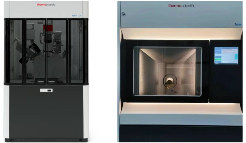
Leveraging advanced microscopy techniques such as Transmission Electron Microscopy (TEM) and Focused Ion Beam (FIB), GRGTEST has systematically developed a suite of solutions for comprehensive internal structure analysis of advanced process chips. This enables the successful, layer-by-layer deconstruction of critical internal structures and material composition – progressing from the package level down to the wafer level.
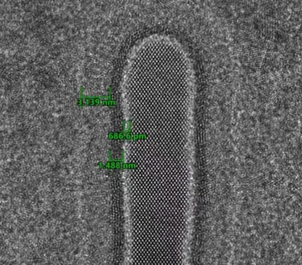
GRGTEST possesses specific wafer-level manufacturing process microscopy and failure analysis capabilities for 3nm and below nodes, including atomic-scale microscopy of structures like FinFETs and GAA (Gate-All-Around). These capabilities allow GRGTEST to offer key services to advanced wafer manufacturers, such as process failure analysis (PFA), FIB ultra-thin sectioning, and high-resolution TEM analysis. Its client base encompasses leading domestic wafer fabs, semiconductor equipment suppliers, panel manufacturers, IC design houses, universities, and research institutes.
As 3nm chips herald a new era for China's semiconductor industry, GRGTEST remains committed to providing full-cycle quality assurance – from atomic-scale inspection to system-level validation – through the professional lens of its "industrial eye."