

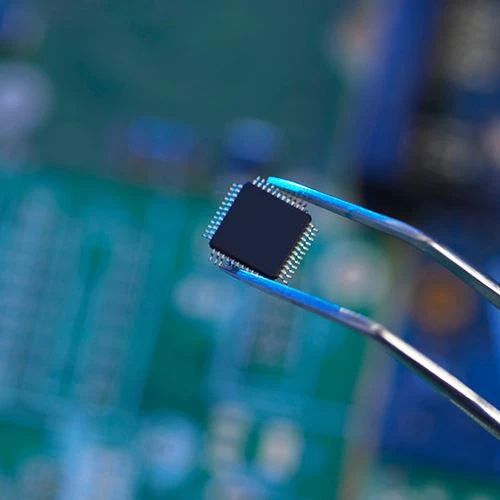
A high-precision Moiré-based substrate warpage measurement system that analyzes light diffraction on sample surfaces. Delivers micron-level deformation measurement with a stable thermal cycling control system. Purpose-built for chip, precision component, and microelectronic packaging reliability assessment. Fully compliant with JEDEC JESD22-B112C, supporting global electronic packaging warpage measurement, especially in high-temperature reflow soldering scenarios.
- ISO/IEC 17025 Accredited
- CMA Certified
- CNAS Certified
- Global Report Recognition
Testing Services
| Test Function | Applicable Samples | Primary Application | Reference Standards |
|---|---|---|---|
| Static Warpage Measurement | PCB boards, electronic components, wafers, thin films, etc. | Room-temperature flatness inspection | JEDEC JESD22-B112A, IPC-6012 |
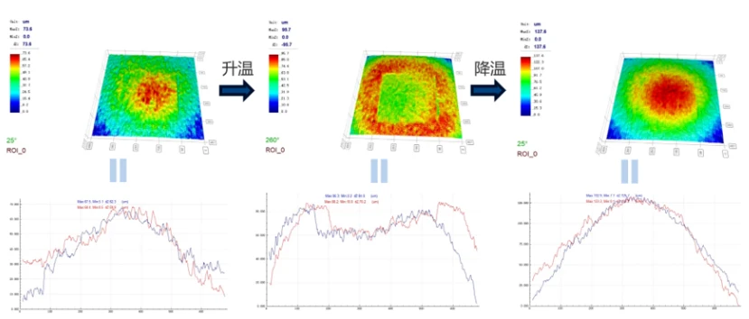
| Temperature-Dependent Warpage Measurement | Thermal stress analysis, reflow soldering simulation | JEDEC JESD22-B112A, IPC-6012 | |
| Dynamic Warpage Measurement | Real-time monitoring during reflow soldering | JEDEC JESD22-B112A | |
| 3D Surface Mapping | Detailed planar analysis, spatial reconstruction | Per customer requirements | |
| Defect Detection | Identification of assembly problem areas | Per customer requirements | |
| Custom Testing | Specific temperature profiles or mechanical preload testing | Per customer requirements |
Key Information
Industries Served
Electronics manufacturing, PCB fabrication & semiconductor packaging, materials science & engineering
Testing Standards
JEDEC JESD22-B112A • IPC-6012
Test Items
Static warpage • Temperature-dependent warpage • Dynamic warpage • 3D surface mapping • Defect detection • Custom testing
Turnaround Time
10 working days (standard); expedited testing available upon request
Service Background
The Moiré warpage testing system addresses the electronics industry's demand for high-precision warpage measurement, particularly for quality control under thermal stress conditions. By delivering a non-contact, high-resolution measurement method, it efficiently assists customers in verifying component flatness, optimizing design and manufacturing processes, and improving the reliability and quality of electronic products.
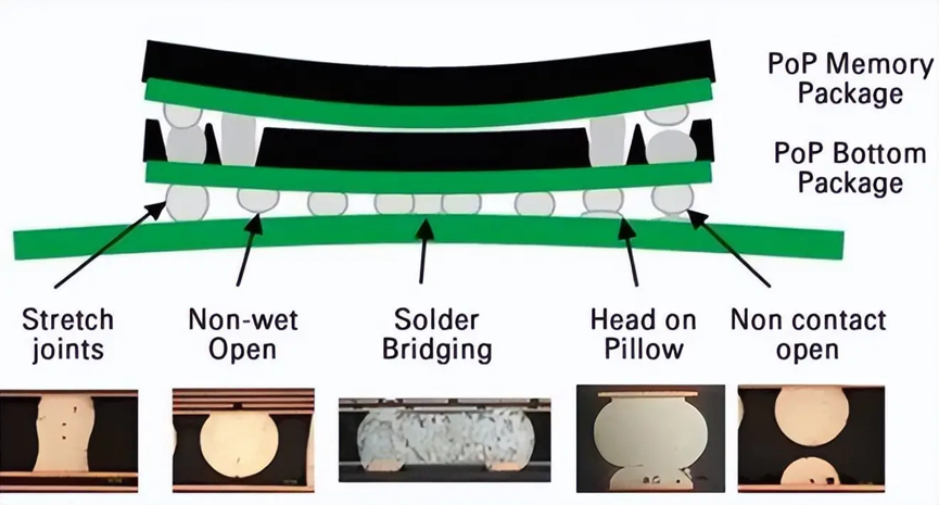
Why Choose Our Testing Services
Comprehensive One-Stop Service
We provide a full-range service spanning component screening, testing, and failure analysis - covering reliability testing, environmental testing, and failure mechanism analysis. This eliminates the hassle of coordinating with multiple vendors.
Extensive Industry Experience
With deep expertise across electronics, automotive, telecommunications, and power industries, we understand component- and PCB-specific failure modes. Our team rapidly pinpoints issues and delivers customized solutions.
Internationally Accredited
CNAS (ISO/IEC 17025) and CMA accredited, with globally recognized test reports. Our certifications help customers meet compliance requirements in both domestic and international markets.

Frequently Asked Questions
What are the resolution and repeatability of Moiré warpage testing?
Gratings are selected based on customer requirements and sample characteristics. For samples smaller than 50 mm, resolution and repeatability reachsub-micron level (<1 µm). For larger samples, resolution and repeatability are within2.54 µm
What sample types are suitable for this test?
Moiré warpage testing is primarily used for smooth, continuous surfaces such asPCBs, BGAs, LGAs, and semiconductor packages. It is also applicable to material testing and biomedical imaging.
What is the temperature range of the testing equipment?
The temperature control system supports testing fromroom temperature up to 280 °Cfor high-temperature measurements.
Please pay attention to safety when using,wait until the power is turned on to warm up before operation
Quick Facts
- Standard: JEDEC JESD22-B112C
- Method: Moiré Interferometry
- Resolution: Sub-micron (<1 µm)
- Temperature Range: RT ~ 280 °C
- Turnaround: 10 business days
- Accreditation: CNAS, CMA
Hot Tags: moiré substrate warpage testing, China moiré substrate warpage testing service provider, corrosion mechanism and fatigue test, material consistency evaluation and thermodynamic, material failure analysis, metal and polymer materials analysis, milling grinding tests, surface insulation resistance sir test


